“The best SPS is its absence.” – not a good joke that the system engineers scare the battered and unhappy pulse converter developers with.1
In the “first grade”, in the previous article, we considered the initial moments of construction of one of very important circuits for power electronics – a single-cyclel forward converter (FC). Two fundamental formulas were given – for capacitance i = C du/dt and for inductance u = L di/dt.
Four rules were formulated: that the capacitor voltage (#1) and the inductor coil current (#2) are constant over a small time interval, that the capacitor (#3) has zero ampere-second area per period, and that the inductor coil (#4) has zero volt-second area per period.
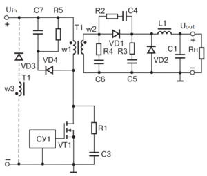
Fig. 1 – Schematic diagram of the power section of a single-cycle forward converter
It is shown that for the simplest circuit of the forward converter (Fig. 1) the transformer magnet wire is remagnetized along a symmetrical hysteresis loop using the maximum possible range of induction (!).
The output filter L1, C1 of the forward converter is an excellent integrator, effectively isolating the average component of the output voltage in accordance with the regulation characteristic Uout = @Uin N2 without losses.
As a result, this Mercedes among other structures of DC/DC converters has a remarkable property – it even without any stabilizing feedback has a very small output resistance, i.e. in relation to the load has very useful properties of a voltage generator (with gapless choke currents).
So, the speed is picked up, let’s keep moving.
The real FC has voltage and current diagrams slightly different from those in the previous article.
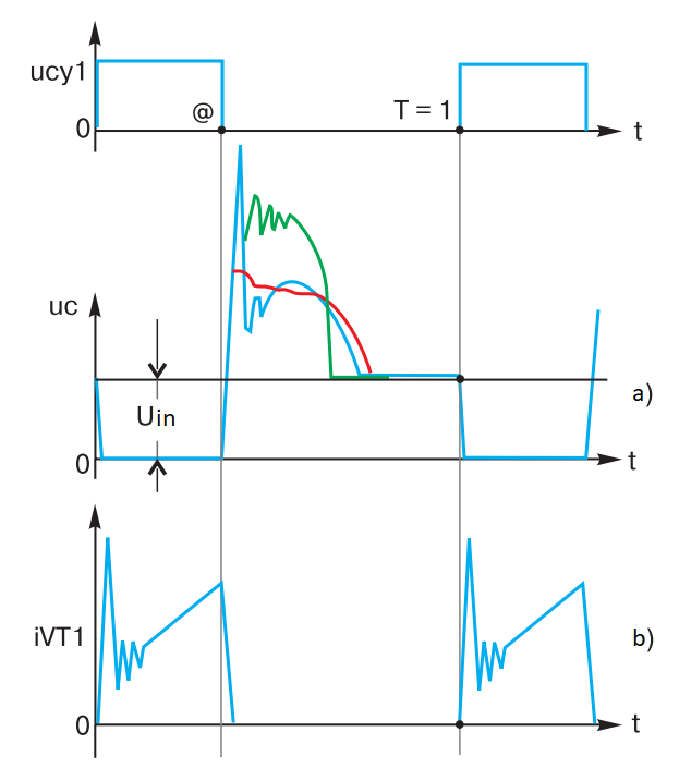
Fig. 2 – The diagrams of voltage and current of the power transistor FC drain
When transistor VT1 is turned off, a narrow spike, sometimes of significant magnitude, many times greater than the input voltage can be observed in the voltage diagram at the drain (Fig. 2a). The real presence of stored energy in the leakage inductance Ls of transformer T1, W = i2Ls/2, causes a voltage overshoot at the drain of transistor VT1 when it is turned off. Since the value of the leakage inductance is small, this process has a short duration, a “needle” is born, as the professionals say. Then, after a short high-frequency transient process a slow resonance process is formed, described in the previous article, called “navel” among common people.
In fact, we are dealing with a double-circuit resonant system, in which the distributed and reduced capacitances of the transformer resonate separately and in combination with the inductances of Ls dissipation and L magnetization. The type of resulting voltages during the resonance processes can be different. Besides clear separation of “needle” and “navel”, one can observe “two-humped camel” and very often asymmetric voltage due to merged “needle” and “navel”, it is like half of a sinusoid with steep leading edge and flat trailing edge (the author hopes that readers will add exotic names of processes in forward converter). We should add that so far we are talking about the diagram shown in blue (Fig. 2a).
When transistor VT1 is turned on, a “horn” – a triangular current overshoot with a high-frequency transient – is observed on the current diagram (Fig. 2b). The appearance of this spike is due to the fact that at the moment of turning on of the transistor VT1 diode VD2 is still in the conducting state, the diode VD1 begins to open, resulting in a short circuit of the output winding of transformer T1. In fact, transistor VT1 is switched to short-circuit transformer T1, as a result of which a large extractor current flows through transistor VT1 for a short time – this terrible “horn” is born. By the way, its magnitude is limited by the dissipation inductance of transformer T1, it is fortunately not short-circuited at this time.
For lovers of subtlety it should be added that there are other reasons for the inrush current when switching on, such as the discharge on the transistor VT1 of numerous previously charged capacitances, such as the capacitance of the transformer, etc.
How do forward converter transistors survive in such terrible conditions of existence, among “needles”, “horns” and “navels”?
First, only MOSFETs survive, with few exceptions. They have unique properties of speed, overload capability, and, most importantly, they have virtually no secondary breakdown phenomenon, which does not allow bipolar transistors to be used reliably in high-frequency forward converter.
Secondly, special circuit solutions are used to protect the transistors.
Circuit R1, C3 briefly takes over the decreasing operating current of winding w1, which allows quickly and elegantly (ie, without losses and overloads) turn off transistor VT1 with a relatively smooth rise in voltage at the drain. Slowing down the rate of change of current w1 at the turn-off stage of transistor VT1 reduces the amount of voltage overshoot at the drain – “needle”; remember the formula for inductance. Unfortunately, you have to pay for everything, here the payback is the additional load of the transistor VT1 at the on stage, because the charged capacitor C3 has to be discharged. The action of the circuit R1, C3 professionals call “shaping the off-path” of transistor VT1.
The dissipating inductance of transformer T1 can also be considered an element of the circuit, often its value in the forward converter, operating at high frequencies, increase the ferrite bead, dressed on the terminal of winding w1 of transformer T1. The role of leakage inductance is twofold. On the one hand, it causes a voltage surge at the drain of the transistor VT1 “needle”, but on the other hand, it does not allow the extract current to develop through VT1 when it is turned on, limiting the “horn” of the current.
The “needle” is dealt with by means of various circuits, e.g. VD4, C7, R5 in Fig. 1. This circuit limits, trims the voltage overshoot, as shown by the red line in Fig. 2a.
Finally, the author cannot skip the circuit recommended in almost all textbooks consisting of an additional winding w3 and a diode VD3. The diagram corresponding to the action of this circuit is highlighted in green.
The idea is simple. If in a DRC-chain such as VD4, C7, R5, the power corresponding to the energy W = i2Ls/2 stored in the dissipation inductance is uselessly dissipated as heat, then due to additional winding w3 through the diode VD3 can be reset, return energy W to the primary power source without significant energy losses, as experts say – recuperate. And it is tempting to cut the “navel” in the same way. Efficiency is not lost, and overvoltage from transistor VT1 is removed.
Unfortunately, it is difficult to implement this idea in a high-frequency converter and it is rarely used in practice. It is very difficult at high frequencies, more than 100 kHz, to ensure good magnetic coupling between windings w1 and w3, for this it is necessary to wind these windings simultaneously. In this case there are difficulties with the breakdown voltage, so complex insulation has to be used. The w1 and w3 windings must have the same number of turns, and this is at odds with the desired variation range of @. And most importantly, introducing an extra winding into the transformer design results in increased Ls dissipation inductance, increased stored energy W, increased initial ejection pulse, etc., i.e., what was fought for…
Additional circuits, such as R4, C6; R2, C4; R3, C5 shown in Fig. 1, are used to reduce the level of noise born in windings, circuit board elements, component pins, etc. due to sudden changes in voltages and currents.
At this point, it is useful for the tired reader to take a break, rest, drink tea, in general, gain strength to continue.
Let’s continue our consideration of the simplest forward converter with the question of voltage and current selection of transistors and diodes.
Let’s look at the diagrams shown in Fig. 2. With a maximum fill factor @, say 0.66, in accordance with rule #4 (volt-second area equal to zero per period), it is easy to assume that the “navel”, if it is prescribed completely (which is the lowest navel height), will be about 1.4 times higher than the input voltage multiplied by 0.66 and divided by (1 – 0.66). Try to do these estimates geometrically. The formula is:
Unav = 1.4Uin min @/(1 – @)
Since Uin min is in effect at this time, the maximum voltage at the drain of transistor VT1 will be Uc max = Uin min + Unav. Let’s take a typical range of input voltage variation multiple of K = Uin max/Uin min, e.g. K = 2. Then
Uc max1 = 3.8Uin max/K = 1.9Uin max
We can take @ = 0.33, which corresponds to Uin max. Here, of course, it is taken into account that we are considering a stabilized forward converter with a constant output voltage. Then, applying rule #4 (the umbilical height will remain the same), we get:
Uc max2 = Uin max + Unav = 2,8Uin max
Of two evils we choose the worst – Uc max2.
Thus, if the “needle” – ejection due to the action of the leakage inductance – was not present, we would already have to choose transistor VT1 at triple the maximum supply voltage. But, unfortunately, the typical “needle” may well be 1.2…1.5 times higher than the “navel”. A voltage reserve of 20…30% wouldn’t hurt (Kres = 1.2…1.3).
The author recommends using the ratio for transistor selection by voltage in the simplest forward converter:
Uc max = Kres (1,4 * 1,5Uin max + Uin max) = 4…5 Uin max
The choice of transistor in terms of current for stabilized forward converter is made on the basis of output power of forward converter Pout, efficiency, input voltage Uin (the slope of the top of the current diagram is not considered).
Average current for the period Ic1 = Pout / (Efficiency × Uin min). The pulse current is obtained by dividing this expression by @, corresponding to Uin min, e.g. @ = 0.66. Then, taking into account the “horn” (Kh = 1.2…1.5), we get:
Ic max1 = (1.2…1.5) Pout K/(Efficiency * Uin max * @max)
For Uin max we can get
Ic max2 = (1,2…1,5) Pout/(Efficiency * Uin max * @min),
of course in this case
@ = @min = @max/K = 0,33
Thus, Ic max1 = Ic max2. There is no choice here.
The author recommends using the ratio to select transistor VT1 by current in the simplest forward converter (typical efficiency = 0.8, and the top bevel must be taken into account, ~1.2):
Ic max = 1,5 × 1,2 Kres Pout K/(Efficiency * Uin max * @max) = 8…10 Pout/Uin max
The esteemed reader understands that one can put up with such a choice of current, given the large current overload capacity of MOSFETs; after all, this is power, due to the pulse principle of operation. But it is not always possible to put up with a very high drain voltage excess ratio in a MOSFET. Imagine that the maximum input voltage is 360 V! (Rectified voltage at the upper limit is ~220 V.) Then MOSFETs with a maximum drain voltage of 1400…1800 V must be used (and there are virtually none!).
By means of noticeable efficiency loss (from 80% to 75…70%) it is possible to cut not only “needle” but also a part of “navel” itself in the simplest PSC. Then maybe Uc max = 2…3 Uin max, although this is also a lot.
Science suggests two solutions here, aimed at reducing overvoltage and increasing efficiency.
The first solution, the so-called “active limitation” means removal of active resistance in the DRC-chain VD4, C7, R5, shown in Fig. 1, and allowing current to flow against diode VD4 in pause (with a small dead time to eliminate through currents) – Fig. 3.
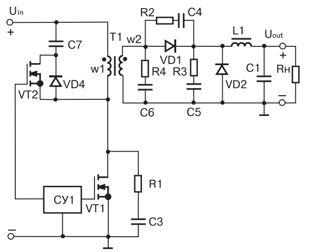
Fig. 3 – A forward converter scheme with active surge limitations
For such a forward converter, a capacitor C7 with a capacitance large enough to make the accumulated voltage of emissions on it more or less constant is chosen.
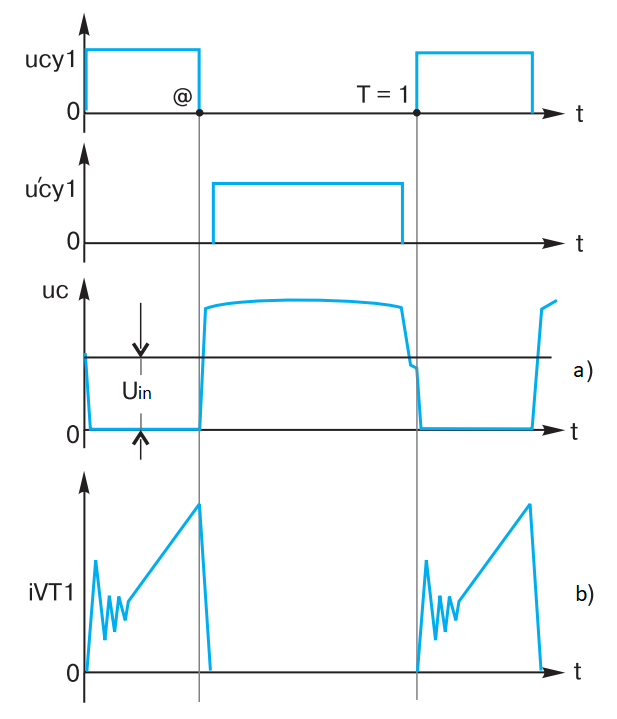
Fig. 4 – Voltage and current diagrams in the forward converter circuit with active limiting
The auxiliary transistor VT2 is switched on with a small delay after switching off VT1 (Fig. 4) and is switched off a little before the main transistor VT1 is switched on. All of the voltage rise energy at the drain of transistor VT1 passes into the energy of capacitor C7, W = C * Uc2/2, as current flows through the circuit – open VD4, C7. The capacitor C7 then passes the stored energy through the open auxiliary transistor VT2 into the winding w1, remagnetizing the transformer T1.
After switching off the additional transistor VT2 the current developed by this moment in the winding w1 and, therefore, led to the accumulation of energy in the leakage inductance Ls of transformer T1, W = i2Ls/2, is now shorted to the reduced capacity of the primary winding w1, which is much less than the capacitor C7. As a result the voltage at the drain of the transistor decreases and can in principle become less than Uin by the time the transistor VT1 is turned on.
The most important thing happens – the overvoltage at the drain of the power transistor (Fig. 4a) decreases sharply. In such a circuit, efficiency losses are small, and the power transistor VT1 is turned on more gently, with less noise – the “horn” of the drain current is reduced.
Another circuit solution is called an “oblique half-bridge”. You can see why it is an oblique bridge from Fig. 5.
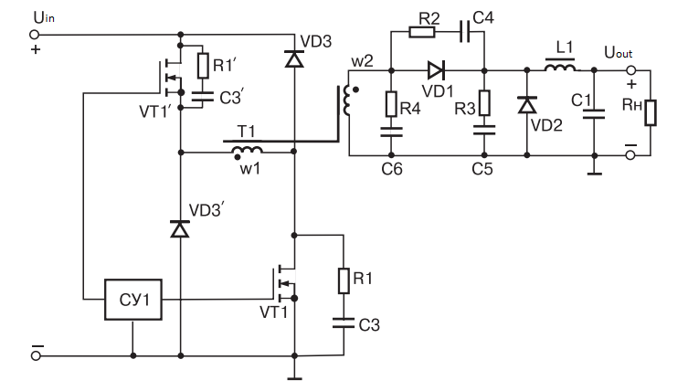
Fig. 5 – Forward converter scheme – oblique half-bridge
In this circuit, the energy of the voltage spikes is recovered into the primary power supply using diodes VD3. This keeps the efficiency high.
But most importantly, this circuit allows the lowest voltage at the drain of power transistors VT1. It does not exceed the supply voltage Uin.
Of course, the esteemed reader understands that the power transistors open and close simultaneously.
The oblique half-bridge circuit is widely used in forward converter designed to operate with higher input supply voltages. This remarkable circuit allows the use of relatively cheap power transistors with a low breakdown voltage. In this case one of its disadvantages – sequential inclusion of two transistors in the path of the operating current of transformer T1 winding w1 – is smoothed by the fact that low-voltage transistors have a reduced open channel resistance, so that large power losses do not occur.
The voltage and current diagrams for the oblique half-bridge circuit are shown in Fig. 6.
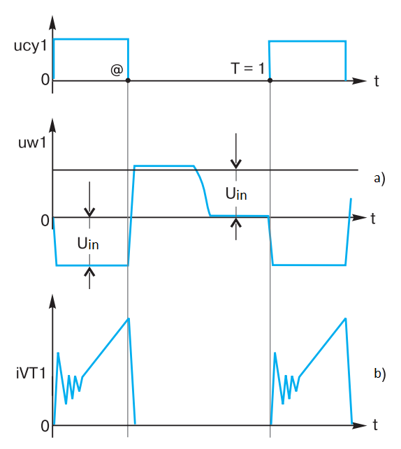
Fig. 6 – Voltage and current diagrams in an oblique half-bridge circuit
The author has cheated a bit here by not giving voltage diagrams for the transistors. Consideration of the voltage on the winding w1 of transformer T1 is suggested because the voltage diagrams on power transistors VT1 may have a different, sometimes bizarre appearance, depending on the symmetry (similarity) of transistors VT1 not only in static, but also in dynamics.
1Author’s Explanation:
1) SPS is a Secondary Power Supply;
2) battered and unhappy – because the system engineers sometimes beat them, because they are sure that the crucial problem in their system is a SPS, even if microprocessors do not count and motors do not spin, the bad one is a SPS;
3) in truth, the author is sure that the SPS was called secondary by evil system designers due to the fact that they always don’t have time to give out input data for power supply design in a timely manner and by that point all convenient design volumes of hardware have already been distributed among their (primary, important) devices;
4) according to importance of consequences for system in case of failure of SPS it is long ago time to rename it to Primary, and qualification of developers of SPS is required very high, here cannot work craftsmen, there should be masters – poets…

