In the “third grade”, in the previous article we reviewed the principle of operation of the car ignition system’s sibling – the most common in the world practice of building pulsed power supplies single push-pull converter (AEC).
The input supply voltage Uin is applied to a series-connected primary winding w1 of transformer T1 and a switch realized on a MOSFET VT1.
When the transistor VT1 is open the primary winding wl of the transformer T1 is connected to the input voltage Uin and energy is stored in the inductance of the winding w1. After closing of the transistor VT1 the stored energy with the secondary winding w2 through the output diode VD1 flows into the load and charges the output filter capacitor C1.
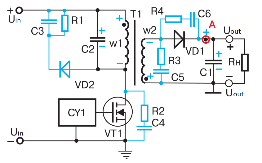
Fig. 1 – Diagram of the power part of the flyback converter
The regulating characteristic of the flyback converter is non-linear:
Uin = Uin * N * @/(1 – @)
where N = w2 / w1 is the transformation ratio of T1, and @ is the fill factor.
In the previous grade, we found two interesting things about the operation of the OOP:
Similarly to forward converter, there are two possible characteristic modes of the secondary winding current w2: the mode of unbroken currents during the pause and the mode of discontinuous currents during the pause of the power transistor VT1. Moreover, in the discontinuous currents mode the flyback converter overestimates the output voltage compared to the value prescribed by the regulation characteristic.
And if the main character, the lord of the rings, in the transformer forward converter is the magnetizing current of the transformer, the main character in the flyback converter is the inductance of the transformer winding. The critical value of the primary winding inductance w1, which determines the boundary between the continuous and discontinuous current modes of the T1 transformer, is:
L1 = Uout * T * (1 – @min)/(2Iout * N2).
From this expression we can see that the smaller the load current, the greater the inductance of the transformer must be provided. Recall that we drew a similar conclusion for the inductance of the output choke of the forward converter. In doing so, we noted that the bursting current mode in flyback converters can be very useful in building high voltage converters.
Finally, we showed that the transformer magnetic core is permanently magnetized, which dictates the necessity of using magnetic core cores with a concentrated or distributed gap.
Of course, a real flyback converter has voltage and current diagrams that differ from the nearly ideal diagrams given in the previous article.
Immediately after transistor VT1 is turned off, a fairly narrow voltage spike, usually of significant magnitude, many times greater than the input voltage, is observed in the voltage diagram at the drain (see Fig. 2a).
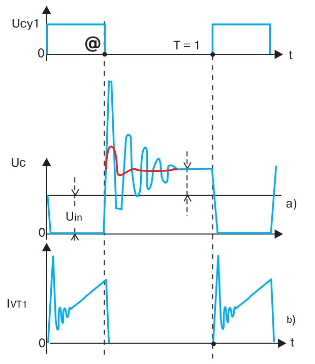
Fig. 2 – Voltage and current drain diagrams of the power transistor flyback converter
The presence of stored energy W = i2 * Ls/2 in the leakage inductance Ls of transformer T1 at switching off causes a resonant transient process at the drain of transistor VT1. Since the value of the scattering inductance is small, this process has a relatively short duration, and the needle ejection is born, as in the forward converter.
However, there are notable differences from the processes occurring in the forward converter.
First, it is easy to notice that in forward converter the output voltage is formed using an integrator, an averaging device – an output LC-filter, i.e., the voltage coming from the output winding during a pulse (forward stroke) is fundamentally greater than the output voltage. And the output winding, accordingly, has the number of turns, adequate to the pulse voltage on the winding.
In flyback converter the output voltage is formed directly from the output winding during a pause (reverse stroke). And the output winding, accordingly, has the number of turns, adequate to the input voltage.
As a result, the number of turns of the forward convertre output winding is always fundamentally greater than the number of turns of the flyback converter output winding.
Here, dear reader fourth-grader, we make a very important conclusion.
If the turns of the primary windings of forward convertre and a flyback converter are the same, the transformation ratio of the flyback converter transformer is always less than that of the flyback converter transformer.
That is, the flyback converter secondary winding has few turns and the flyback converter has a larger difference between the turns of the transformer’s primary and secondary windings than the forward converter. This results in much worse winding magnetic coupling conditions in the flyback converter and, as a consequence, a greater inductance of the transformer primary in the flyback converter.
Therefore, in the flyback converter the throw energy W is greater than the energy in the forward converter, and the needle voltage throw at the drain of the transistor VT1 is always higher and longer in duration than in the forward converter!
Second, the damped needle overshoot in the forward converter occurs around the input supply voltage line and then along the “navel” shape. In flyback converter, the damped needle ejection oscillations occur around the output voltage reduced to the primary winding, i.e., around the supply voltage line plus the reduced output voltage.
The result: with the same transformer design, the initial parasitic voltage overshoot at the power transistor drain is significantly greater in level and energy than the same overshoot in the flyback converter.
On the current diagram in Fig. 2b, when transistor VT1 is turned on, as well as in forward converter, “horn” – a triangular current overshoot with a high-frequency transient process is observed. The appearance of this outlier is due to the fact that the transistor VT1 is usually turned on at a significant voltage at its drain, i.e., the transistor VT1 has to discharge to itself a high-capacitance C2. And the output diode VD1 is still in conducting state, as a result, when you turn on transistor VT1 is a short circuit of output winding of transformer T1 to the output capacitor C1. But for this case the magnitude of the extratok is fortunately limited by the leakage inductance of transformer T1.
To protect the power transistor of the flyback converter from breakdown and from destructive overcurrent, only MOSFETs should be used in the first place. They have unique dynamic characteristics and overload capability. Most importantly, they have virtually no secondary breakdown phenomenon, which does not allow bipolar transistors to be used reliably in high-frequency forward converter’s.
In addition, special circuit decisions are made to protect the transistors by voltage and current. Circuit R1C3 briefly takes over the decreasing operating current of winding w1, which allows fast and elegant (i.e., without losses and overloads) turn off transistor VT1 with a relatively smooth rise in voltage at the drain. Slowing down the rate of change in the winding current w1 at the turn-off stage of transistor VT1 reduces the amount of needle voltage rise at the drain (remember the formula for inductance). The payoff for this positive action is the additional load of transistor VT1 at the on stage, because the charged capacitor C3 has to be discharged. Thus, with the help of the R1C3 circuit, the turn-off path of transistor VT1 is formed.
The leakage inductance of transformer T1 (sometimes even a parasitic phenomenon helps!) can also be considered a circuit measure, because its effect in flyback converter’s operating at high frequencies is often supplemented by a ferrite bead, etc., dressed on the terminal of winding w1 of transformer T1. After all, the role of leakage inductance is twofold. On the one hand it causes voltage rush at the drain of transistor VT1, and on the other hand it causes extracurrent through VT1 when it is turned on, limiting current rush.
The “needle” is dealt with by means of various circuits, e.g. VD2, C3, R1 in Figure 1. This circuit limits, trims the inrush voltage, as shown by the red line in Figure 2a.
Additional circuits such as R4C6, R2C4, R3C5 are used to reduce the level of noise generated in the windings, circuit boards, component pins, etc. due to sudden changes in voltages and currents.
In general, the main thing is that there are quite a few prerequisites for certain efficiency losses in flyback converter compared to forward converter’s.
Think about it.
So, after a little rest, let’s talk about the choice of power transistor.
Let’s continue our consideration of a simple flyback converter with the question of voltage and current selection of transistors and diodes.
Let’s look at the diagrams shown in Figure 2. No matter how we cut off the parasitic voltage rise at the drain of power transistor VT1 using various circuits, we must still keep in mind that in series production it may reach 10-20% of the total supply voltage and the output voltage applied to the primary winding.
At the maximum supply voltage, when the minimum pulse duty cycle is in effect, according to Rule 4 (volt-second area equal to zero per period), it is easy to calculate:
Uout = Uin.max * @min / (1 – @min)
and
Uc.max = Uin.max + Uin.max * @min / (1 – @min) = Uin.max / (1 – @min)
Also write down the relation for the flyback converter (check if it is deduced from the regulation curve) as @min = @max / (@max * (1 – K) + K).
When designing voltage converters, it is common to first set the maximum fill factor value. For transducers with low input voltages, let’s take 0.66, for example. Then the minimum fill factor at twice the supply voltage change (K = 2) will be in accordance with the non-linear control characteristic equal to 0.5. The esteemed reader can also do the calculations geometrically, using rule number #4.
Then Uc.max = 2 * Uin.max
Thus, if there were no “needle” – ejection due to the influence of the inductance of the rescission, then we would already have to choose transistor VT1 at twice the maximum supply voltage. Then we take 10 – 20% for needle overshoot and 20 – 40% voltage margin, to ensure the necessary reliability. As a result, for a flyback converter with a typical double supply voltage change we get:
Uc.max = Kres * (1.1…1.2) * 2 * Uin.max = (2.7…3.4) * Uin.max = (3…4) * Uin.max
The choice of transistor current for the stabilized forward converter is made on the basis of output power of flyback converter Pout, efficiency, input voltage Uin (the slope of top of current diagram is not considered yet).
Average current for the period Ic1 = Pout / (Efficiency * Uin.min). The pulse current is obtained by dividing this expression by the corresponding Uin min, e.g. @max = 0.66. Then, taking into account the “horn” (Kh = 1,2…1,5) we obtain Ic.max1 = (1,2…1,5) * Pout * K / (Efficiency * Uin.max * @max). For Uin.max we can get Ic.max2 = (1.2…1.5) * Pout / (Efficiency * Uin.max * @min), in our case @min = 0.5. Having made the necessary calculations, for K = 2 we obtain Ic.max1 is greater than Ic.max2. Here we choose Ic.max1.
The author recommends using the ratio to select transistor VT1 by current in the simplest flyback converter (typical efficiency = 0,8, and the bevel of the top must be taken into account, and it is about 1,2):
Ic.max = (1.2…1.5) * (1.2…1.4) * 1.2 * Pout * K / (efficiency * Uin.max * @max) = (7…10) * Pout / Uin.max.
One can put up with such a choice of current, given the large current overload capability of MOS transistors, after all it is the energy, due to the pulse principle of operation. But it is not always possible to put up with a large voltage overshoot factor at the drain in the forward converter. Imagine that the maximum input voltage is 372 V! (rectified at the upper limit of +20% voltage of 220V). In this case, you have to use MOSFETs with a maximum drain voltage of 1116…1488V, which theoretically have noticeably worse speed and channel resistance properties than lower voltage transistors and, most importantly, which are virtually non-existent!
Usually by significantly reducing the efficiency (from 80% to 75 – 75%), and this is completely unnecessary extra heat and overloading the input power source, significantly increase the power of the R2C4 and R1C3VD2 circuits. Also use sophisticated transformer winding techniques to reduce leakage inductance. As a result, they reduce the needle pickup at the transistor drain to 2 – 5%.
This reduces transistor voltage requirements by at least 20%. In our unrealistic network case, 893…1190V appears. Already better, because can pass the transistor with voltage 900 V, and such transistors with satisfactory characteristics produces several companies.
Further help in this direction of solving the problem comes only with the option of reducing the maximum fill factor. For mains power supplies under the flyback converter scheme, @max = 0.4 – 0.5 is usually used. Then we can recommend:
Uc.max = Uin.max / (1 – @min) = Kres * (1.02…1.05) * 1.4 * Uin.max = (1.7…2) * Uin.max.
This is a realistic case, since we can use commonly available 700V transistors. Although note, that for efficiency the work with smaller pulse fill factors is not the most joyful thing – the losses grow.
But how to reduce the parasitic voltage overshoot without reducing the efficiency, how to use the energy of this overshoot for peaceful purposes?
Here the dear reader will remember the wonderful circuit, considered in the second grade.
This is the same oblique half-bridge, but for the forward converter (see Fig. 3).
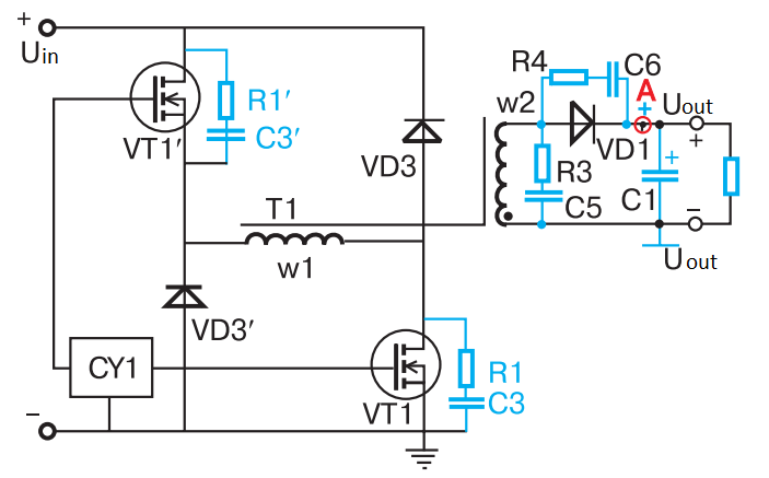
Fig. 3 – The flyback converter scheme – oblique half-bridge
In this circuit, the energy of parasitic voltage spikes is recovered into the primary power supply using diodes VD3. That allows to keep high efficiency.
And most importantly, this circuit allows the lowest voltage at the drain of power transistors VT1. It does not exceed the supply voltage Uin. Of course, the esteemed reader understands that the power transistors must open and close at the same time.
An oblique half-bridge circuit can be effectively used in flyback converter’s designed to operate with higher input supply voltages. As we pointed out earlier, this remarkable circuit allows the use of relatively cheap power transistors with a low breakdown voltage. In this case, one of its drawbacks, i.e. the serial inclusion of two transistors in the path of the w1 winding of transformer T1, is smoothed by the fact that the low-voltage transistors have a reduced open channel resistance, so there are no big power losses.
I.e. flyback converter or forward converter. Look at the roads (better to temporarily move overseas for that). Both are driven, and sometimes Peugeots are even more common than Mercedes.
Here is the question too, dear reader, take your time answering it.
Let’s make some comparisons.
In terms of the maximum voltage across the power transistor for a single push-pull voltage converter, unless the wonderful oblique half-bridge circuit is used, you need:
Uc.max = (4…5) * Uin.max for forward converter and Uc.max = (3…4) * Uin.max for flyback converter.
I.e. here Peugeot is noticeably ahead. In terms of maximum current Ic.max = (7…8…10) * Pout / Uin.max they are practically identical.
Our Peugeot (flyback converter) and Mercedes (forward converter) are on a par with each other in terms of the possibility of using an oblique half-bridge circuit.
Of course, schematically, the flyback converter is simpler than the forward converter. Especially when in popular magazines there is only a simplified power part, so there are five or six elements. Then it is striking that there is no output choke in flyback converter! Of course, this is good, there are less winding elements. However, in a real circuit, which always contains more than a dozen components, dear reader, do not take schemes from advertising articles! – quantitative difference in the components of flyback converter and forward converter is leveled.
Further investigation of this detective point leads to the following comparisons and questions.
What is better: to have two coil elements, each optimized by electromagnetic and structural parameters due to the fundamental possibility of separating the functions of the transformer and choke into different components for flyback converter, or to have an under-optimized transformer on a bad for transformer choke magnetic core and simultaneously have a choke, which is clearly hampered by transformer attributes in the forward converter?
What is better for reliability: to have a whole garland of aluminum (but very cheap) or at best tantalum or ceramic (but both are insanely expensive) capacitors in flyback converter or to significantly reduce the number of output capacitors, shifting a significant share of the filtering function to the output choke in forward converter?
Which is better for mass production: to coil only one multi-winding component or to bother with winding two dissimilar ununified components?
Further arguers can add here that it is much easier to realize a wide range of input voltage variation with flyback converter, others can argue that the path of energy flow during conversion is shorter and straighter in forward converter (maybe that is why it goes straight?) and, consequently, the efficiency is slightly higher, etc., and so on.
The author’s scientific and manufacturing experience has sternly demonstrated that:
In advance, a priori, when selecting the structure of a single-cycle voltage converter, it is impossible to give preference to forward or flyback converter, focusing only on the energy characteristics: current, voltage, power, efficiency.
You understand, otherwise most people would drive only Mercedes or only Peugeot.
It is necessary, in every particular case, to consider both options in detail. And take into account not only voltages, currents, powers, ranges of their changes, behavior of energy characteristics in the predicted critical and transient modes.
It is necessary to consider the subtleties of production technology, the design principles incorporated in the product, heat transfer conditions, layout options, restrictions on the choice of operating frequency, the need or harmlessness of splitting large-sized winding components into parts, low-profile requirements, and much more.
Thus, the choice can only be made taking into account a variety of specific conditions and constraints, in some cases structural and technological and manufacturing plan, rather than electrical and scientific.
Well, what about the recommendations of some scientists, who cite the boundary of applicability of flyback and forward converters in the form of a pointing power division?
The author (smiling) thinks that the flight of scientific thought is not limited…
I must congratulate you, if you carefully, with a pencil in hand, studied the materials of all four lections, made your calculations (and sometimes revealed small bloopers author, for example, the voltage factor when selecting a forward converter transistor in one of the formulas should not be 2.8, but 2, 4) – You have finished Elementary School and are moving on to fifth grade without exams.
Next, in the next lections, we will talk about more thoughtful, but no less interesting and fascinating moments of professional solutions in the field of pulse DC/DC converters.
But that will be Middle School now.

