“The main thing is to explain where the electrons run away…”
Over the past 10 years, the element base of DC/DC converters has changed a lot, new materials have appeared. And the main thing is that the ideas about the expediency of using certain circuits to obtain the specified parameters have changed. Categorical approach prescribing usage of strictly definite structures for definite types of power supplies has disappeared. The influence of economic and market factors on the choice of a converter circuit has increased. All this has made possible what seemed paradoxical and even wrong yesterday.
Here are a few examples:
And so on… Let’s smile (:
In general, the world of power sources has become more diverse.
So it is necessary all the time to study the experience accumulated by mankind, and sometimes to question the most categorical statements. It becomes clear that an educated person can be considered a person who is constantly learning, and not just once received a diploma.
By the way, the author has long unsuccessfully tried to find out why the typical calculations of high-frequency transformers prescribes the use of the concept of dimensional power and why the current density in the wire is set. In reality, any, even quite tiny transformer does not “understand” what the power is, it “understands” what its Curie point is and just feels the heat, which may be different depending on its cooling system. You can set the optimum current density of 2…3 A/mm2 according to the typical table of the calculation manual, and in practice see how well the copper wire in a high-frequency transformer works with the current density 20…30 A/mm2 and more (half a coil, one coil, etc.).
Let’s start consideration of pulse converters with one of very important for power electronics circuit of forward converter (FC) (Fig. 1). This is the most energy efficient power supply structure, a kind of Mersedes Benz (if one likes, then BMW) among other DC/DC converter structures. By the way, surprisingly little described in the literature. Apparently, pro developers working with straight-through converters do not consider it necessary to share “subtleties” (just like Mercedes developers). Blue highlighted elements, which will be considered in further, a closer look at the DSD.
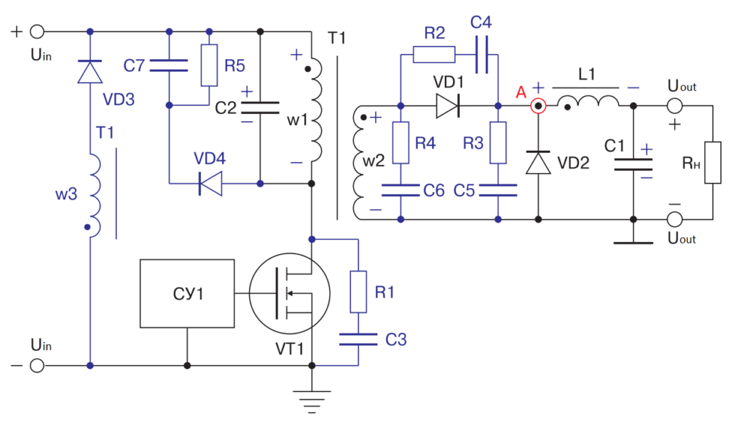
Fig. 1 – Schematic diagram of a forward converter
The input supply voltage Uin is applied to the primary winding w1 of transformer T1 and the switch realized on transistor VT1 connected in series. Assume that the switch on the MOSFET is ideal, it switches quickly from on to off and vice versa. The voltage drop across the on MOSFET is vanishingly small. The Uin source is also good, it is stable, high-frequency, the high-frequency pulse currents of the converter are easily shorted through it. For AC, you can assume that the +Uin and -Uin terminals are equipotential! But with the elements. C2 and w1 are not so simple.
The capacitor C2 is (to some approximation) the equivalent capacitance of all capacitances given to the primary winding w1 of transformer T1:
etc., up to the capacitance deliberately supplied by the designer.
In general, the capacitance of capacitor C2 always exists, and for high frequency converters it cannot be neglected. The w1 winding is in first approximation an inductor coil.
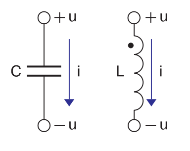
FIg. 2 – Capacitor and inductor currents and voltages
For capacitance and inductance (Fig. 2) the most important laws are expressed in two easy to remember formulas.
For capacitance: i = C du/dt
and for inductance: u = L di/dt.
The first formula tells us that rapid voltage changes on a capacitor of capacitance C will result in very large currents through the capacitor. Trying to “instantaneously” apply a voltage spike to the capacitor (even a very small one) will result in an infinite current surge, which in practice is impossible, since the source of applied energy is finite in its capacity.
Rule #1 – the capacitor “resists” voltage changes on it, reacting by current surges, so the capacitor voltage can be changed only slowly, smoothly. If the current (charge or discharge) through the capacitor is constant at any time interval, then the voltage across the capacitor changes linearly. The second formula shows that rapid changes in current in the inductor coil L will result in very large voltages across that coil. Trying to “instantaneously” change the current in the inductor coil (even by a very small amount!) will result in an infinite voltage spike response, which in practice is impossible, since that voltage will penetrate any insulation.
Rule #2 – the coil “resists” changing the current in it by reacting with voltage surges, so the current through the coil can only be changed slowly, smoothly. If the coil voltage is constant at any time interval, the current through the coil changes linearly. Since an ideal coil has zero resistance to direct current, a constant voltage across the coil cannot exist for long. Since the capacitor has a gap between the shells, a direct current cannot exist in the capacitor for a long time, an infinite voltage will accumulate and the capacitor will break down. Hence two more rules, illustrated in Fig. 3.
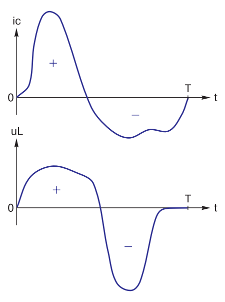
Fig. 3 – Ampere-second characteristic of a capacitor and volt-second characteristic of an inductor
Rule #3 – in the case of a stationary periodic process with period T, the ampere-second area of the capacitor for period T is zero.
Rule #4 – in the case of a stationary periodic process with period T, the volt-second area of the inductor coil for period T is equal to zero. That is, the areas marked “+” and “-” must be strictly equal.
To the delight of lovers of all sorts of “fiddlesticks”, a transformer is not one coil, but at least two. It has a magnetic core, which has magnetic field strength H and induction B. Which of these is primary and which is secondary is a confusing question, about the same as with the concepts of current and voltage. In general, there is “both. If we imagine that in a coil with the number of turns w current I is flowing, then in a closed magnetic wire with the length of the middle line l the magnetic flux H = w I/l is generated (Fig. 4).
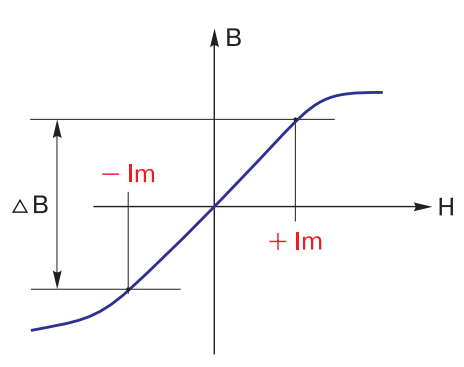
Fig. 4 – Magnetization curve of transformer
As a result, induction B is developed in the core. This (as well as H) is the evidence of magnetic flux which goes through the windings w1 and w2 and gives rise to an EMF equal to the primary winding voltage w1, if the number of windings w1 and w2 are the same (if the number of windings are different, it is proportional to the ratio of the number of windings).
Here begins the most confusing and incomprehensible. If the primary winding is closed to the input voltage source, and the secondary to the transformer load, the currents I1 and I2 give rise in the core to magnetic fluxes that destroy each other! What a meanness. Fortunately, in the primary winding (primary in relation to the direction of energy passing!) there is always an additional, often very small current, io, which is the magnetizing current. This is what magnetizes and remagnetizes the core! This is the “main character” of the transformer. Without this, the transformer just doesn’t work. It is this current that makes the core of the transformer move along the magnetization curve. That is, with the same windings w1 and w2 I1 = I2 (Fig. 5), and the magnetization of the transformer does not depend on whether the operating current is 1 A, 10 A or even 100 A through the windings.
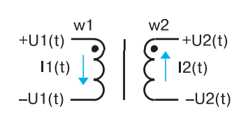
Fig. 5 – Currents and voltages in transformer windings
All the same, the operating currents create mutually destructive magnetic currents. What matters is what io will be. And the magnetizing current io is determined by the above formula for inductance, i.e. the primary inductance L and the magnitude and form of the voltage applied to the primary: io = 1/L u dt. If the voltage applied to the primary winding is constant, io will increase linearly according to the sawtooth law.
Attention! While in a normal inductor coil the current cannot change by a step change, the operating current in either winding of a transformer can, if there is a current jump in the other winding, to maintain the total magnetic flux in the core. In other words, in an inductor coil in a transformer the operating current can “jump” from one winding to the other!
The most important calculated relationship in a transformer is: U1 I1 = U2 I2. This follows from the fact that the efficiency of the transformer is practically unity. U2/U1 = I1/I2 = w2/w1 = N – is the transformation ratio.
This is enough for the first time.
Let’s continue looking at the operation of the RPM.
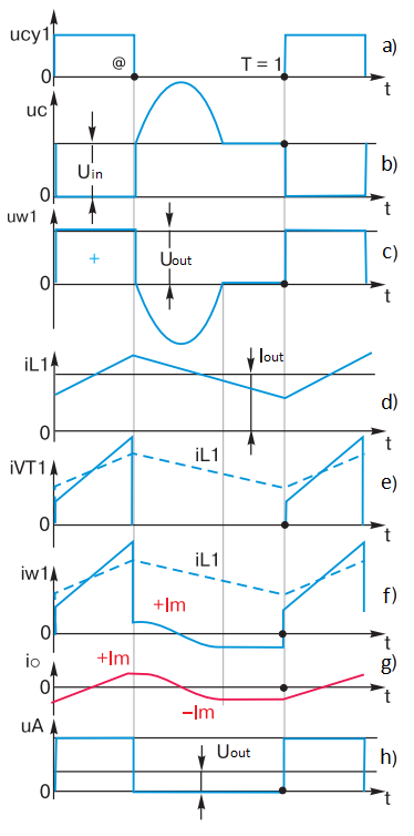
Fig. 6 – Control pulses from the control circuit
The control circuit of cy1 delivers control pulses to the gate of MOSFET VT1 (Fig. 6a), which are sufficient to reliably open transistor VT1. The pulse repetition period is T. The duration of each pulse is Ti = @T, where @ is the pulse fill factor. In relative units, taking the period as one, T = 1, @ will be the relative pulse duration. By the way, why the author denoted the pulse width as “dog” rather than the commonly used “gamma” will be explained in the following articles.
With transistor VT1 open the primary winding of transformer w1 is connected to the input voltage Uin. A typical oscillogram at the drain of transistor VT1 is shown in Fig. 6c. During the time @ there is a constant voltage Uin on the winding w1 and the capacitor C2 (Fig. 6c). The polarity of the transformer windings and capacitor C2 is shown in Fig. 1.
At the secondary of the transformer w2 for @ there is the same form of voltage Uw2, having a magnitude according to the transformation ratio.
During @ there are rectangular pulses at point A, where only the positive part of the voltage passes through. Assume that the capacitance of capacitor C1 is large enough to neglect the voltage ripple on it, hence the voltage on the load is stable and constant. It is obvious that the voltage applied to the choke L1 is the difference of the amplitude of the rectangular pulse at point A and the constant voltage on the load.
According to the formula for inductance, the current through the choke L1 increases linearly over time @ (Fig. 6d). Since the choke current flows through winding w2 at this time, the same increasing current exists in winding w1 as well. In other words, for the time @ the current of transistor VT1 increases linearly (Fig. 6d, 6e), and this increase is primarily caused by the rising current of the choke L1 (thin blue line in Fig. 6d, 6e).
In addition, as mentioned above, when a constant voltage is applied to the transformer’s primary winding w1, magnetizing current io will increase in it, and its magnitude can be calculated from the formula for inductance. Therefore, Fig. 6d, 6e shows a steeper “bevel” of the pulse top than that caused by the current buildup of the choke L1.
When transistor VT1 is turned off during @, there are instantaneous (at first approximation) and smooth processes.
The turn off and current decay of transistor VT1 is “instantaneous”. Conditionally instantaneous (correct, very fast) discharges capacitor C2 to zero, because at this point in time it gives a large operating current to winding w1 (i.e. it briefly acts as a source of input voltage). Closing of the direct diode VD1 can also be considered as instantaneous due to removal of a signal from the transformer winding w2 and “jumping” of operating current (it is the current of choke L1) from the secondary winding w2 to the bypass diode VD2. Further in time the choke current will short-circuit through VD2.
The process of current flow through the choke L1 is also smooth – the current simply does not change. And most importantly, at this point will be unchanged and the magnetizing current io transformer, which flows through the primary winding of the transformer w1 as through the “pure” inductance Lm and can not change by leaps and bounds. Therefore, Fig. 6e shows that at time @ the current in w1 jumps down to a positive value of +Im.
After the time @ the voltage on the winding w1 changes its sign (Fig. 6c). This happens because the magnetizing current io of the transformer smoothly starts to recharge capacitor C2, so the polarity of the voltage on capacitor C2 and on winding w1 changes its sign. At this time the direct diode VD1 is closed, and as a result the whole output part of the OPT is disconnected from the transformer (transistor VT1 was disconnected even earlier). The transformer becomes “free” and is a high quality oscillating system. Let’s represent the transformer as a resonant oscillating circuit of the primary winding inductance L and the capacitance of the capacitor C2. Since there is a current Im in the inductance of the winding L at time @, this current forms half of a sinusoid (Fig. 6c), overcharging capacitor C2. The base duration of this “half” of the sinusoid will always be constant, since it is half the frequency period of the resonant circuit L-C2.
Of course, the same, but negative sign half of the sine wave will be on the secondary winding of w2. At this time, a constant voltage equal to the output voltage of the FC is applied to the choke L1 (the voltage drop on the bypass diode VD2 is neglected). According to the formula for inductance, the current in L1 decreases linearly (Fig. 6d). It can be seen that as a result of a periodic repetition of processes, the current of the choke L1 is continuous and has a sawtooth shape. Since in the steady-state process constant current cannot flow through the capacitor C2 (rule #3), we conclude – the average current of the choke L1 is always the load current I out. If w1 equals w2, then we can mentally draw the choke current with its true value on the graphs – Fig. 6d, 6e (dashed line).
Let’s return to the sine wave. If transistor VT1 were no longer switched on after the moment @, the sinusoid (resonance process) would continue long enough, slowly decaying as the losses in the windings, capacitor C2 and the core of transformer T1 are small. However, the “attempt” of the sinusoid (as if it were alive!) to cross the abscissa axis and “exhibit” positive polarity leads to a positive voltage on winding w2 (as in Fig. 1), and the direct diode VD1 begins to open. As a result, both diodes VD1 and VD2 will open, with their small differential resistances they actually shunt winding w2 and further, through the magnetic coupling in transformer T1, also winding w1. Therefore, after the passage of the first half-wave of the sinusoid on the voltage graph on the windings w1 and w2 appears a peculiar horizontal “shelf”, lasting until the time T.
Well, what happens to our main character, the “lord of the rings” (the author means the closed configuration of the magnetic circuit) – magnetizing current io?
As already mentioned, it generates a resonance process after the time interval @. The current io recharges capacitor C2 to its maximum value – the sinusoidal amplitude – and then, due to the fact that capacitor C2 begins to give charge to the winding inductance w1, and this current begins to flow through w1 in the opposite direction. This variable behavior of io is easily explained by the formula for inductance – if the voltage on the inductor coil is a sine wave, the current is a cosine wave (Fig. 6g). The current io passes through zero when the voltage sine has a derivative equal to zero. It is easy to assume that when the quality factor of the L-C2 circuit is large (or, as they say, when the damping decrement is small), the initial current -Im is equal to the final current -Im (Fig. 6g) (the voltage derivatives are equal and opposite in sign).
Then, when, due to the above short-circuiting of the winding w1, the sinusoid “ends”, there is a “conservation” of the current -Im until the time T = 1. What is “conservation”? Recall that for an LR-circuit the time constant is not the usual t = RC (as for a capacitor), but t = L/R. That is, when R tends to zero, the time constant increases dramatically, tending to infinity. This means that if the inductor coil, through which the current flowed, is short-circuited, the current will be stored in the coil for a very long time – canned!
Thus, dear reader, we have proved step by step that at the beginning of transistor switching on the magnetizing current has a negative value, equal in absolute value to the positive value Im at the moment of the end of the open state pulse of transistor VT1. And this is serious already. There is a remarkable, new to us phenomenon – no matter how long the operating pulse is, the magnetizing current will find the middle of the pulse itself and exactly in this magic place will cross zero (Fig. 6g) opening!
For more serious (in terms of age) readers will be interested in the author’s conclusion.
The magnet wire of the transformer in the above forward converter is remagnetized by a symmetrical hysteresis loop, using the maximum possible range of induction (Fig. 4). Of course, with the above assumptions and a certain intention of the pulse converter builder. For now, let’s put this conclusion among our paradoxes (many textbooks claim otherwise).
At point A (Fig. 1) there are rectangular pulses (Fig. 6h), each of which is actually the supply voltage at the input Uin, transmitted through a transformer and straight diode VD1, which has a very small differential resistance. Given that the bypass diode VD2 (open during the pause phase of VT1) also has a very low differential resistance, we can say that point A is the “conditional” output of the voltage generator. In this case the output filter L1, C1 can be considered as an integrator, which separates the average component from the pulse voltage. This is how the output voltage is formed on the load Uout = @UinN (this, by the way, is called the regulation characteristic). It is easy to see that if the input voltage and transformation ratio N are constant, the output voltage can be changed by changing the pulse fill factor @.
Since there is almost no loss in this integrator, it can be seen that the FC has the remarkable property that it has a very small output resistance even without any stabilizing feedbacks, i.e. in relation to the load it has very useful properties of a voltage generator (hence the “Mercedes”).
All of the above regarding the output voltage is true as long as the current of the choke L1 is unbroken. Notice in Fig. 6e. If to decrease a current of load I out, the saw-tooth curve of a current of choke L1, not changing under the form, will fall lower and lower, until will not touch by the bottom peaks of an axis of abscissa, i.e. the current of choke L1 in the bottom peaks will equal zero. This mode of choke L1, and all RPM is called a boundary mode, till this moment condition Uout = @UinN is satisfied.
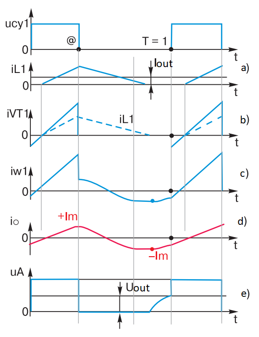
Fig. 7 – Diagrams of currents and voltages in the elements of forward converter with unbroken choke current
A further decrease in load current will lead to the fact that on a curve of current of choke L1 there will be areas with zero current – “breaks” (Fig. 7a). In Fig. 7b, 7c are diagrams of currents through the transistor VT1 and through the winding w1. As a result of the current gap of the choke L1, i.e. from the moment when the current of the choke L1 becomes equal to zero (i.e. when the bypass diode VD2 closes), the short circuit w2 through VD1 and VD2 will disappear, and the current io will no longer be “conserved”. The absolute value of io will start to decrease up to the time T = 1, Fig. 7e. Therefore, the opening of transistor VT1 will occur at a lower absolute value of current -Im, and the current io will increase during the open state of transistor VT1 to a larger value +Im. All this will lead to a shift of the core magnetization trajectory upwards and its approach to the saturation area. This is a negative phenomenon, because when the core is saturated the losses in the transformer increase sharply and the current (now non-linear) of transistor VT1 rises sharply – and then a lot of trouble can happen in the FC. The voltage at point A (Fig. 7d) before the point T = 1 acquires a characteristic “chipping”, or resonance process appearance. Naturally (as can be seen in the graph – Fig. 7d), the output filter loses its integrator abilities, as the output voltage rises and at the same value of @ becomes greater than the average value of the pulse sequence at point A in Fig. 6з. In the limit, when the load current tends to zero, the integrator L1C2 together with VD1 (VD2 closed) degenerates into a peak detector. In this case the voltage at the output of the PSC is equal to the amplitude of the pulses on the winding of w2: Uout = UinN. Of course, the output resistance of the FC in this mode increases sharply (this is no longer a Mercedes), and the converter loses the properties of a voltage generator. It remains to be noted that all this ugliness is called the discontinuous current mode. To shift the boundary of discontinuous currents to lower load currents, the inductance of choke L1 must be increased. It is easy to derive from the formula for inductance: Ldross = UoutT (1 @min)/(2Ioutmin).
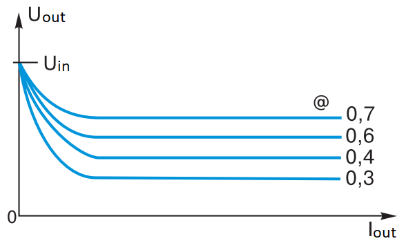
Fig. 8 – Diagrams of currents and voltages in the elements of FC with a breaking current choke
It is easy to notice that at Iout = 0 Ldross = ∞, i.e. such a choke would have to be wound for “a very, very long time”. The only way out is the additional boost of the forward converter. Figure 8 shows the horizontal sections of the output voltage curves as a function of Iout and @ parameter, as well as the effect of the output voltage “hiking” when the load current decreases due to the gap current mode of the choke L1.
The inquisitive reader, of course, replaced the excessive categorical attitude to the gap current mode with the very one, which was ironically mentioned at the beginning of the article. I’ll tell you a secret: if you want, you can find golden grains of great qualities in the mode of discontinuous currents, but this is already the last classes of elementary school… The author assumes that by this point many readers are quite tired. Therefore, other interesting properties of the forward converter (including the purpose of the mysterious circuits highlighted in blue in Fig. 1) are in the next article. In the next grade.

