 en
▼
en
▼
“Two tank crewmen – two cheerful friends…”*
*The cheerful crewmen friends were known to be a bit more, but that’s not the point. Try pedaling a bicycle with one foot. Not very poetic? Two is certainly more capable, more power – it moves faster.
In the previous articles (grades) we have practically already considered the most important basics of building pulse transducers. We could consider that the elementary school is over and we, together with the reader-pupils, are moving on to the secondary school. However, there are several sections in this applied science, without which it would be a bit difficult to apply the obtained knowledge in practice. Therefore, there is a proposal to study a little more. And then move on to high school and then to higher school.
Let’s outline the next movement in our education within the elementary school.
In fifth and sixth grade, we’ll go over dual and push-pull converters, in seventh we’ll go over zero voltage and zero current converters, and if there are opportunities, in eighth we’ll talk about interference and thermal problems.
So, what have we learned about the most common pulse converters – forward converter and flyback converter, not without intention designated by us as a kind of Mercedes and Peugeot (the author hopes that readers have saved the magazine numbers of the previous articles – grades)?
We know that in forward converter the functions of galvanic isolation, transformation of voltage and current and the functions of filtering, conversion of everything pulsed to analog are clearly separated between the transformer and the choke. In flyback converter, these functions are basically combined in one element, the choke-transformer.
We have deduced that in the flyback converter transformer choke can remagnetize along a symmetric hysteresis loop, using the maximum range of induction, while in the flyback converter transformer choke is under the action of a unidirectional magnetic field and is permanently magnetized.
The “Lord of the Rings” in the forward transformer is the magnetizing current, while the forward converter transformer (choke) has a protagonist – the inductance of the windings. The regulating characteristic of the forward converter is linear, while the flyback converter is non-linear, although this is not a bad thing, because the same changes @ in the flyback as in the forward converter lead to large changes in the output voltage. That is, the flyback converter is regulated more broadly with less effort.
We have made an important conclusion, that it is impossible to give preference in advance, a priori, to forward or flyback converter, being guided only by power characteristics.
It is necessary to take into account not only voltages, currents, powers, ranges of their changes, behavior of energy characteristics in the predicted critical and transient modes. We will have to consider the subtleties of production technology, design principles incorporated in the product, heat transfer conditions, layout options, limitations on the choice of operating frequency, the need for or harmlessness of splitting large-sized winding components into parts, low profile requirements and much more.
An objective choice between forward or flyback converter can be made only by taking into account a variety of specific conditions and constraints, in some cases of a design-technological and manufacturing nature, rather than electrical and scientific ones.
Speaking with a smile – we couldn’t find out which is better, Mercedes or Peugeot. But we found out a universal circuit with a not quite serious name – oblique half-bridge which appeared to be a wand and a wand of choice for both converters – forward and flyback – in cases when even unique features of MOSFETs in terms of speed, overload capability and absence of secondary breakdown do not help – in cases of work with high input voltages.
Here the attentive reader might ask – why do we need tankers and a bicycle? The point is that in this class we will talk about dual single-cycle voltage converters, in which the analogy with two pedals (two arms, two legs, etc.) can be seen.
Why is it necessary to double pulse voltage converters? Certainly not just to increase the power in the load. Let’s look at the problems of increasing the frequency of pulse converters as a means of miniaturization from the perspective of the element base.
The most difficult to increase the frequency for power transistors. Imagine that every time a power transistor is turned on, it almost instantly discharges its own capacitances associated with its drain, almost instantly discharges (charges) all the capacitances of the structure connecting the drain to the power buses. There are also extract currents caused by moments of short circuits in the magnetic circuits when the output diodes are switched, etc. As a result, once per period, the power transistor experiences significant current overloads when turned on. Naturally, with increasing frequency the power transistors have more and more difficulty, which is manifested in the form of more and more heating (loss of efficiency). This is not far from the trouble – failure.
But the easiest way to increase frequency are reactive elements, transformers, chokes, filter capacitors, for the sake of reducing the size of which the increase in frequency is conceived. By the way, with an excessive increase in frequency, heat losses increase so much that the increasing volume of required cooling systems makes all these efforts senseless. In other words, there is some optimal frequency value, above which it is harmful to rise.
The usefulness of solutions is obvious, when by increasing the number of power transistors working once per period, but with a time shift, provides an increase in the frequency of pulse processes in the reactive elements. That is, the power transistors operate at a low frequency, and most of the reactive elements operate at a high frequency (in this case – double).
This solution is a particular and most common case of multi-phase voltage converters – in fact, we are considering two-phase converters. The fundamental difference between dual converters and so-called push-pull converters is the use of two transformers instead of one.
Let’s take a look at the diagrams of a dual forward converter and a dual flyback converter, shown in Figures 1 and 2.
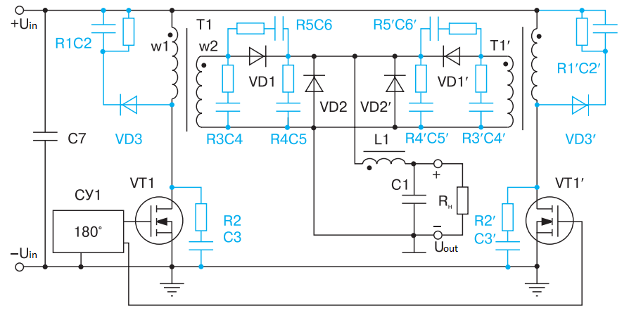
Fig. 1 – Diagram of the power part of the forward converter
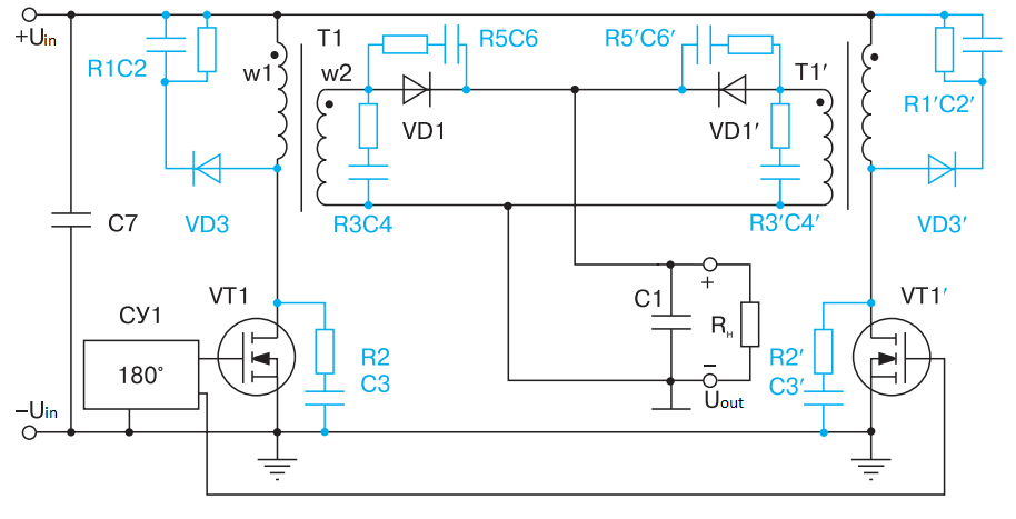
Fig. 2 – Diagram of the power part of the flyback converter
The first circuit consists of two combined outputs of the forward converter. The power transistors of the converters are controlled by a push-pull control circuit, which operates at twice the frequency and feeds a sequence of pulses to the gate of the power transistors with an offset of 180 degrees.
In fact, during one switching period of each power transistor all elements of the converter are activated only once, i.e. operate with the same frequency. Exceptions are bypass diodes VD2 and VD2 with their chains and most importantly – elements of output filter L1, C1, and elements of input filter (conventionally shown as capacitor C7), which work at double frequency.
As a result it is possible to significantly reduce the volume of output and input filters and improve the miniaturization performance of the converter with increased output power.
The theory of such converters shows that shifting the pulse control sequences of power transistors by 180 degrees corresponds to the most optimal filtering process in the output filter.
The closest analogy from life is a bicycle drive with two legs working in turn.
The inquisitive reader will of course propose to combine diodes VD2 and VD2` with their chains into one unit, as well as elements C2, R1 and C2, R1` accumulating and dissipating the emission energy, and in most cases he will be right. In general, dual converters give a lot of room for the designer’s ingenuity. Try, for example, to link the transformers of a dual converter so that each one helps the other to demagnetize. As a result, if you are lucky, you will repeat many of the dozens of registered patents in the field yourself.
Similar reasoning applies to the circuit in the Figure 2.
Only here the output filter capacitor C1, as well as elements of the input filter (conventionally shown as a capacitor C7) work at the doubled frequency. However, dear student, you should also understand that the filtering work of the output inductance of transformers of single inverse-going converters is also facilitated to provide the mode of continuous currents in consideration can no longer take the whole period, but only half of it!
It should be taken into account that the voltage diagrams on the power elements of dual converters can differ significantly from those of single converters. This is explained by mutual influence of single converters as a part of a dual converter.
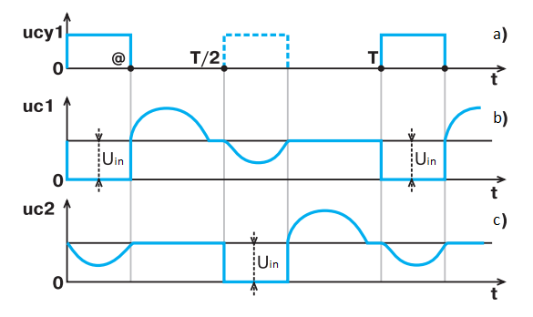
Fig. 3 – Voltage diagrams at the power transistor drains of the dual forward converter according to the scheme of Figure 1
For example, Figure 3 shows the diagrams for a dual forward converter made according to the diagram in Figure 1. We can notice that after the dome-shaped ejection has passed the “navel” and a “shelf” has formed at the level of supply voltage (this process is described in detail in the first article, “first grade”) a dome-shaped ejection is formed below the supply voltage after the time T/2. This happens because from the moment of time T/2 the power transistor of the second forward converter turns on, and the short-circuit mode on the secondary winding of the transformer of the first forward converter is eliminated. Similarly, the operation of the first forward converter affects the operation of the second forward converter.
Depending on the ratio of the duration of operating pulses and the duration of resonance processes, which determine the type of dome-shaped pulses, in practice we can observe a bizarre variety of voltage forms at the power transistor stacks.
This beauty has a downside as well – various instabilities can arise in closed-loop converters. Experienced designers in such cases say – additional feedback loops have appeared.
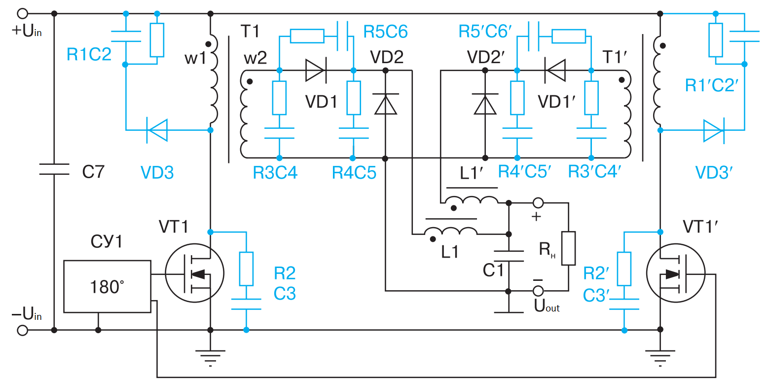
Fig. 4 – Modified scheme of the power part of the dual forward converter
Therefore, the circuit modification shown in Figure 4, in which only the output capacitors are combined, is used. Due to the separate output reactors, the influence of the single converters of the dual forward converter is significantly reduced. Here, dear student, you should feel (of course, if you are not a C), that besides the work of the output capacitor C1 at the doubled frequency, the work of output chokes L1 of forward converter’s single converters is also facilitated – to provide the mode of unbroken currents, you can take into account not the whole period, but only its half.
The operation of single converters as a part of dual based on oblique half-bridge schemes (see Fig. 5) is organized in the same way.
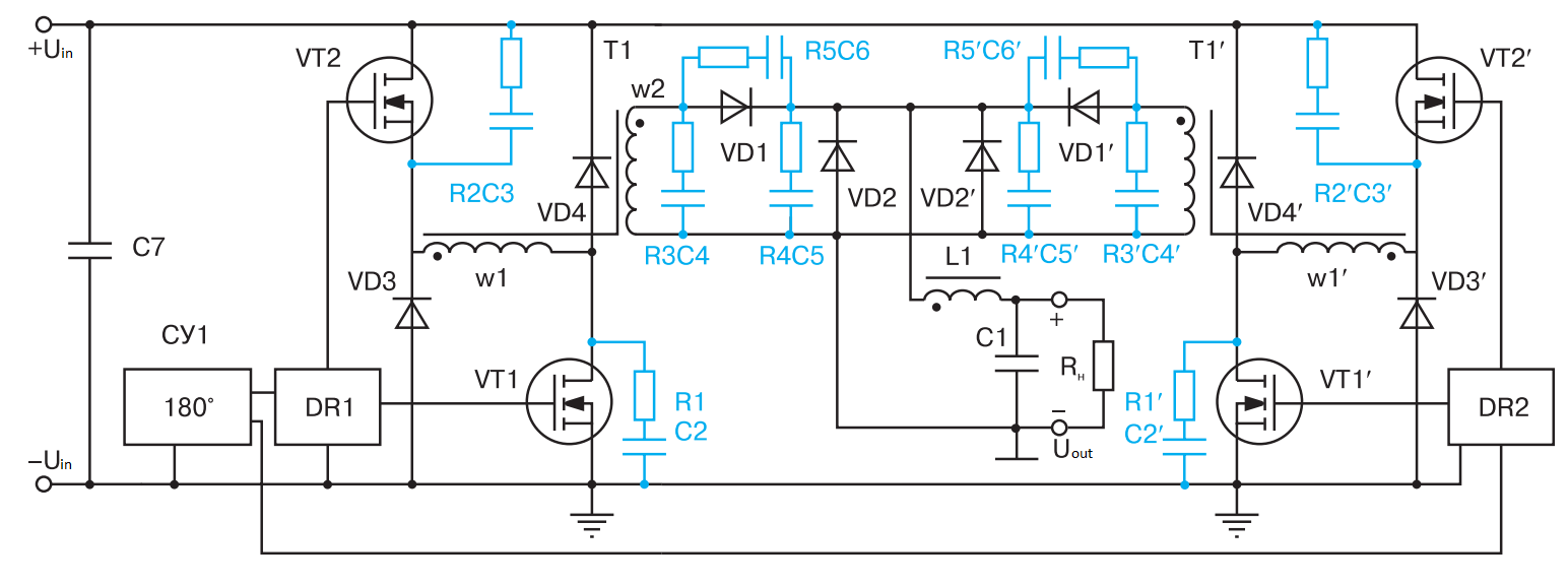
Fig. 5 – Schematic of the power part of the dual forward converter based on the oblique half-bridge structure
Here, two forward converters based on a remarkable oblique half-bridge circuit are combined to form a dual forward converter according to the variant with a common output choke.
The power capabilities of such a solution can be judged by the Japanese Lambda converter, which is on the author’s desk at this night and inspires the writing of an article about dual converters. On the front panel of this very compact device (volume about 4 dm3) there are output parameters 5 V, 600 A (!).
Of course, the esteemed reader-student remembers from the first grade materials that the remarkable circuit of the oblique half-bridge is good because, firstly, the voltage on the power transistors does not exceed the value of the input supply voltage. Secondly, the energy stored in the transformer core and in its leakage inductance is not converted into useless heat, as it happens in the simplest single-cycle converter circuits, but is successfully recovered into the input power supply.Although it is clear that for such positive properties of the push-pull half-bridge you have to pay with double the number of power transistors and a more complicated control circuit.
However, in dual push-pull converters there is a unique opportunity to get all the advantages of oblique half-bridge and to avoid the drawbacks.
Let’s consider the circuit in Figure 6.
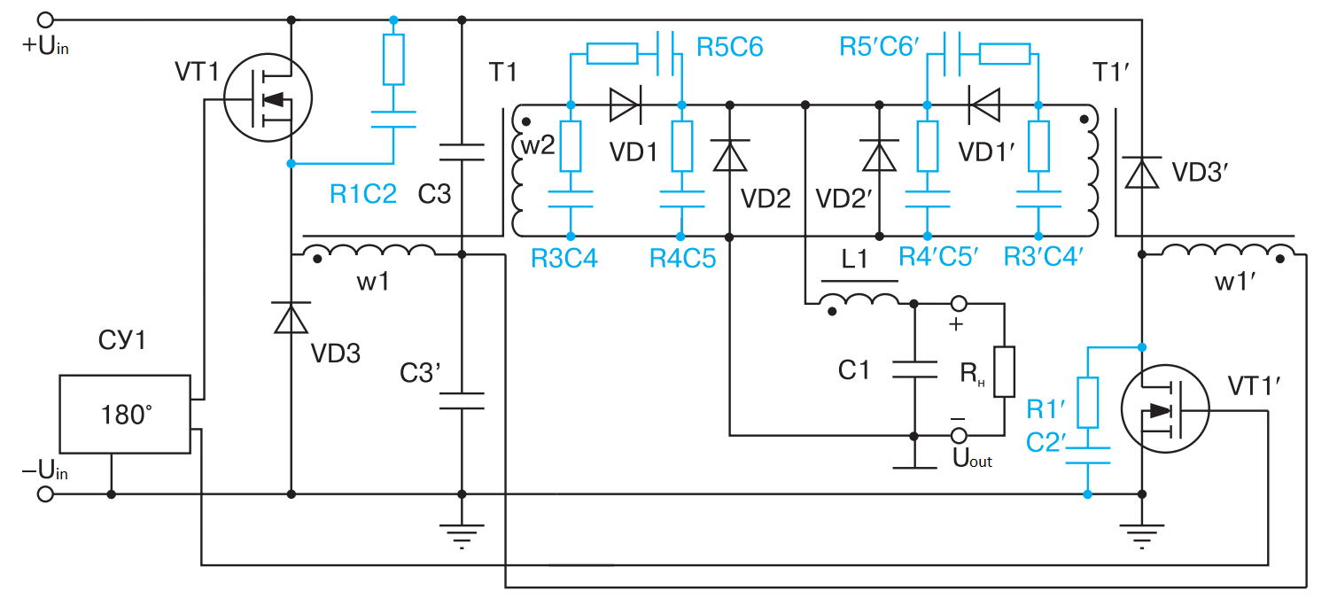
Fig. 6 – Schematic of the power part of a dual forward converter based on a capacitive divider structure
The capacitive divider based on the capacitors C3 and C3` is actually an element of the input filter. With sufficient capacitance of these capacitors they can be considered as input voltage sources for single forward converter, combined into a dual converter.
The full duty cycle of the first forward convertrer consists of an open and a closed phase of the power transistor VT1. In the first phase the power supply of the first single converter is carried out from the capacitive divider on capacitors C3 and C3`. At the same time C3 is discharged and C3` is charged.
In the second phase of the process, the electricity stored in the core of transformer T1 is recuperated into capacitors C3 and C3`. At the same time C3 is also discharged and C3` is charged. As a result, the voltage at the midpoint of capacitors C3 and C3` rises slightly.
The complete cycle of the second forward converter consists of an open state phase of the power transistor VT1 and a closed state phase. In the first phase of this process from the same capacitive divider C3 and C3` the second single converter is powered. At the same time, C3 is charged and C3` is discharged. Accordingly, in the second phase of this process, the electricity stored in the core of the transformer T1` is recuperated into the capacitors C3 and C3`. At the same time C3 is charged and C3` is discharged. As a result, the voltage at the midpoint of capacitors C3 and C3` decreases slightly. The described processes are repeated in subsequent periods. Figure 7 shows a dual flyback converter scheme based on similar principles.
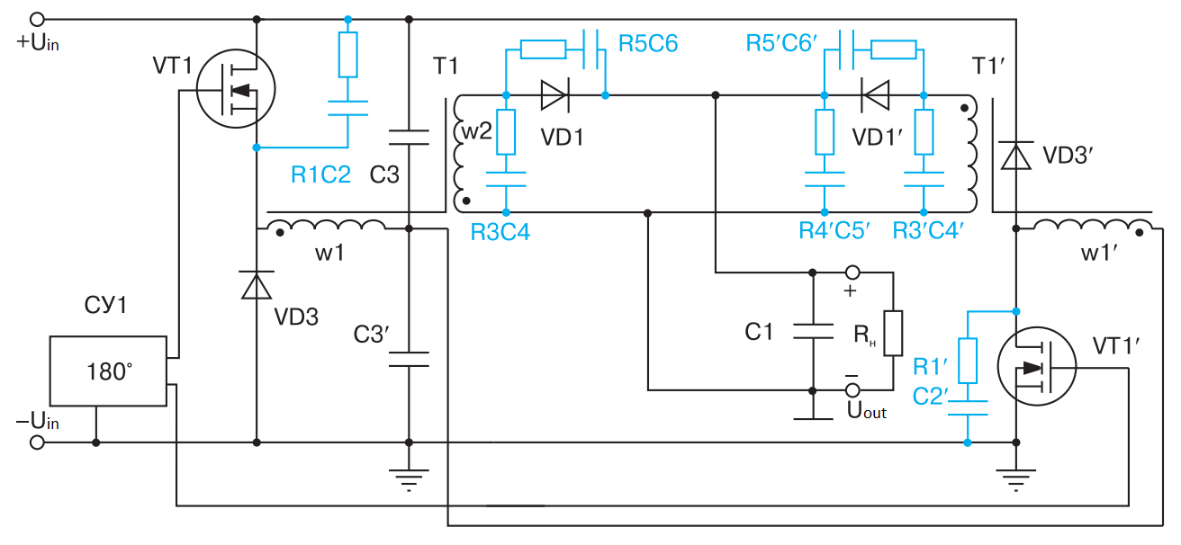
Fig. 7 – Schematic of the power part of a dual forward converter based on a capacitive divider structure
Since we have not yet given voltage diagrams for the dual flyback converter, we shall show and comment on them for this particular case (see Fig. 8).
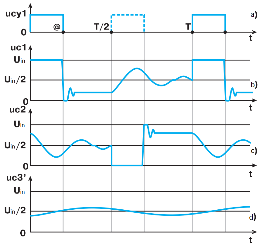
Fig. 8 – Voltage diagrams at the power transistor drains of the double flyback converter based on the capacitive divider structure
The voltage at the drain of transistor VT1 in its open state for a time interval from 0 to @ is equal to the input supply voltage Uin. After the transistor VT1 is closed, there is a brief voltage drop down due to the dissipation inductance of the transformer T1. However, when trying to form a negative voltage at the drain of transistor VT1 after time @ the internal diode of this transistor opens and the voltage is fixed. After a brief parasitic resonance process at the drain of the transistor VT1 the voltage is set below the line Uin/2 by the value of Uout`.
From about time T/2 a state is established at which all the energy stored in the inductance of the transformer T1` has already been transferred to the output capacitance C1 and the load. There is a free resonance process up to the moment T. The voltage (uc2) diagram at the drain of transistor VT1` is similar to that shown for transistor VT1, only it is shifted by half of period T.
Let us consider in detail the operation of the capacitor chain of capacitive divider C3 and C3`. The drain current of the power transistor VT1, when it is open, passes from top to bottom in the circuit through the capacitor C3`, charging it. Naturally, at this time the capacitor C3 is discharged. Then, after the closure of transistor VT1, the energy stored in the dissipation inductance of transformer T1 is transferred to capacitors C3 and C3`, while C3 is also charged and C3` is discharged.
Since the power transistor VT1` is schematically at the bottom and connected to the bus Uin, all the diagrams for transistor VT1` are similar to those for transistor VT1, taking into account their shift by T/2 and flipping by 180 degrees in the vertical plane.
When the second single transistor converter on VT1` works, the drain current flows down the circuit through the capacitor C3, charging it. Naturally, at this time the capacitor C3` is discharged. Further, after the closure of transistor VT1, the energy stored in the dissipation inductance of transformer T1`, is transferred to capacitors C3 and C3`, while C3 is also charged and C3` is discharged.
As a result, the voltage at the midpoint of capacitors C3 and C3` has the form of small oscillations relative to the line Uin/2.
So, the fifth class has been passed. In the sixth we will look at popular two-cycle converter circuits. I wonder, dear reader-pupils – is the knowledge increasing?
